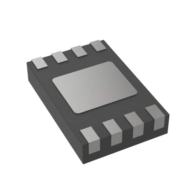
AD9173BBPZ - High-performance 16-bit 12.6 GSPS dual-channel RF DAC
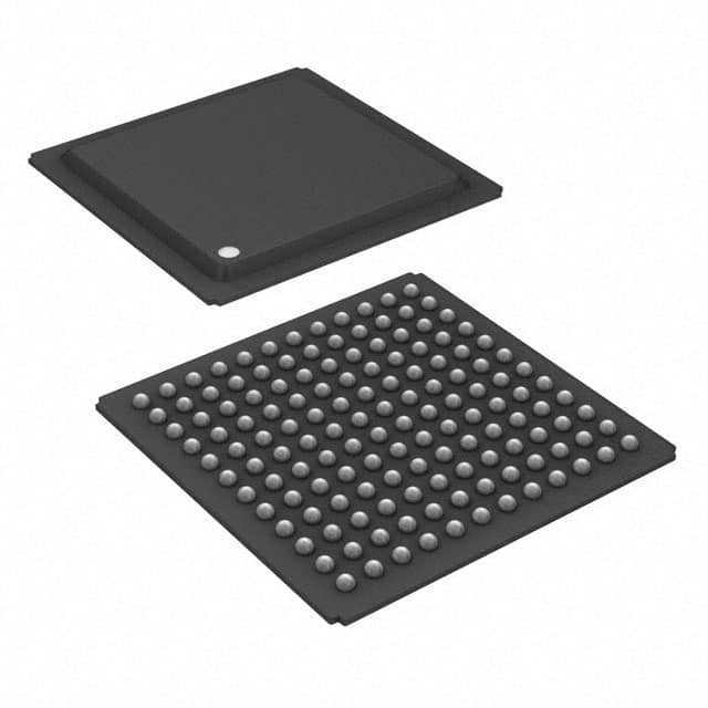
- Part No.:
- AD9173BBPZ
- Manufacturer:
- Analog Devices Inc.
- Package:
- 144-FBGA
- Description:
- IC RF DAC 144BGA
- Quantity:
- Payment:

- Shipping:

Article Details
- Details
- Specifications
- Comparison
Introduction
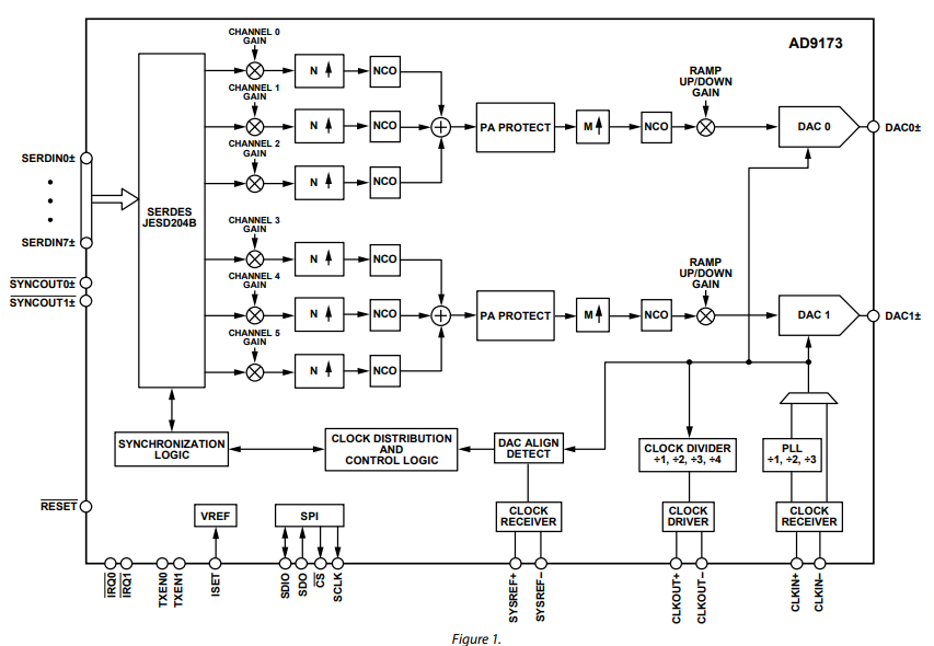
The AD9173BBPZ is a high-performance dual-channel 16-bit digital-to-analog converter (DAC) from Analog Devices, packaged in a BGA-144 (10x10) format. It can achieve a sampling rate up to 12.6 GSPS. This device integrates an 8-channel, 15.4 Gbps JESD204B data input interface, a high-performance on-chip DAC frequency multiplier, and digital signal processing capabilities for single-band and multi-band direct radio frequency (RF) wireless applications. It is highly practical for applications in wireless communication infrastructure, instrumentation, and automated test equipment.
Features
- Supports multiband wireless applications
- 3 bypassable, complex data input channels per RF DAC
- 1.54 GSPS maximum complex input data rate per inputchannel
- 1 independent NCO per input channel
- Proprietary, low spurious and distortion design
- 2-tone IMD = −83 dBc at 1.8 GHz, −7 dBFS/tone RF output
- SFDR < −80 dBc at 1.8 GHz, −7 dBFS RF output
- Flexible 8-lane, 15.4 Gbps JESD204B interface
- Supports single-band and multiband use cases
- Supports 12-bit high density mode for increased data throughput
- Multiple chip synchronization
- Supports JESD204B Subclass 1
- Selectable interpolation filter for a complete set of input data rates
- 1×, 2×, 3×, 4×, 6×, and 8× configurable data channel interpolation
- 1×, 2×, 4×, 6×, 8×, and 12× configurable final interpolation
- Final 48-bit NCO that operates at the DAC rate to support frequency synthesis up to 6 GHz
- Transmit enable function allows extra power saving and downstream circuitry protection
- High performance, low noise PLL clock multiplier
- Supports 12.6 GSPS DAC update rate
- Observation ADC clock driver with selectable divide ratios Low power
- 2.55 W at 12 GSPS, dual channel mode
- 10 mm × 10 mm, 144-ball BGA_ED with metal enhancedthermal lid, 0.80 mm pitch
Electrical Characteristics
DAC Performance- Resolution: 16 bit
- Maximum update rate: 12.6 GSPS
- Complex input rate: 1.54 GSPS (11-bit) / 1.23 GSPS (16-bit)
- Ultra-wideband mode rate: 3.08 GSPS (11-bit, 16-bit SERDES) / 3.4 GSPS (11-bit, 12-bit SERDES)
- Dual-tone IMD: −83 dBc @ 1.8 GHz, −7 dBFS
- SFDR: < −80 dBc @ 1.8 GHz, −7 dBFS
Interface
- JESD204B interface: 8-lane, 15.4 Gbps per lane, Subclass 1
- Number of data channels: 3 bypass complex input channels per RF DAC
- NCO: 48-bit per channel, supports frequency synthesis up to 6 GHz
- Interpolation filtering: Channel interpolation 1×~8×, final interpolation 1×~12×
Power consumption
- Typical power consumption: 2.55 W @ 12 GSPS dual channels
- Package: 144-ball BGA_ED, 10×10 mm, 0.8 mm pitch
- Operating temperature: -40°C ~ +85°C
- Please note the layout of high-speed signals, analog outputs, power isolation, and heat dissipation pads
Application
- Wireless communication infrastructure
- Multi-band base station radio frequency system
- Microwave/E-band backhaul system
- Instrumentation, automated test equipment (ATE)
Typical Application Components
- JESD204B High-Speed Interface: FPGA → Differential Line Pair → AD9173 JESD Rx
- Clock Input: High-frequency low-jitter clock source → Clock Buffer → DACCLK/REFCLK
- SYSREF Synchronization: Clock Chip → SYSREF → FPGA & AD9173
- RF Output: DACOUTP/N → Balun → Matching Circuit → RF Link
- Power Supply: Multiple LDO/PMIC Provide 1.0V, 1.3V, 1.8V
- Control Interface: SPI Interface for Configuration Control
PRODUCT HIGHLIGHTS
- Supports single-band and multiband wireless applicationswith three bypassable complex data input channels per RFDAC at a maximum complex input data rate of 1.54 GSPSwith 11-bit resolution and 1.23 GSPS with 16-bitresolution. One independent NCO per input channel.
- Ultrawide bandwidth channel bypass modes supporting upto 3.08 GSPS data rates with 11-bit resolution, 16-bitSERDES packing and 3.4 GSPS with 11-bit resolution, 12-bit SERDES packing.
- Low power dual converter decreases the amount of powerconsumption needed in high bandwidth and multichannelapplications.
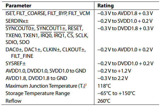
Absolute maximum ratings
Working principle
The core working principle of AD9173 is as follows: It receives high-speed digital IQ data through the JESD204B interface → performs digital up-conversion and interpolation processing → outputs high-linearity signals directly in the radio frequency band using a 16-bit high-speed DAC. The main workflow is divided into four parts: digital front-end → digital up-conversion → DAC output stage → RF output.1. Digital Front-End
The external FPGA or baseband processor transmits high-speed IQ digital data through the 8-lane JESD204B interface into the chip.Each channel supports up to:
- 1.54 GSPS complex input
- Based on 11/16-bit SERDES packing
2. Digital Channel Processing
AD9173 contains 3 bypassable complex data channels for each RF DAC. Each data input channel includes configurable gain stages, interpolation filters, and channel numerically controlled oscillators for flexible multi-band frequency planning.3. Internal Clock System
AD9173 has a high-performance low-noise PLL that can multiply the external reference clock to generate the required high-speed clock for the DAC.4. DAC Core
The data after digital up-conversion enters the high-speed DAC- Resolution: 16-bit
- Fastest update rate: 12.6 GSPS
- Output is in current-mode differential signal
- The RF output is achieved through external Balun and matching circuits
5. RF Output Stage
The DAC output is a high-speed differential current signal, which is processed by the external network:- AC coupling capacitor
- Balun (converts differential to single-ended)
- Filter (low-pass or band-pass)
- Driver power amplifier (PA) or test instrument front-end
Conclusion
The AD9173BBPZ is an ultra-high-speed dual-channel 16-bit RF DAC that supports a sampling rate of up to 12.6 GSPS and is equipped with an 8-lane 15.4 Gbps JESD204B interface, enabling faster data throughput and system bandwidth. Each channel features 3 complex input paths and independent NCO, facilitating the generation of multi-frequency bands and wideband signals, among other advantages. With its internal NCO, interpolation filter, multiple data channels, and PLL clock system, the AD9173 can directly generate high-frequency, wideband, and low-distortion RF signals, significantly simplifying the wireless transmission architecture.
- Product attributes
- Attribute value
- Manufacturer:
- Analog Devices Inc.
- Series:
- -
- Package/Case:
- 144-FBGA
- Packaging:
- Bulk
- Part Status:
- Active
- Resistance:
- Not Verified
- Tolerance:
- RF DAC
- Composition:
- Surface Mount
- Features:
- 144-BGA-ED (10x10)
- Temperature Coefficient:
- -
- Operating Temperature:
- -
- Supplier Device Package:
- Power (Watts):
- Wireless Infrastructure
- Ratings:
- Size / Dimension:
- Height - Seated (Max):
- Number of Terminations:
- Failure Rate:
| Image |  |
 |
| Part Number | AD9173BBPZ | AD9173BBPZRL |
| Manufacturer | Analog Devices Inc. | Analog Devices Inc. |
| Series | - | - |
| Package/Case | 144-FBGA | 144-FBGA |
| Packaging | Bulk | Tape & Reel (TR) |
| Part Status | Active | Active |
| Programmable | Not Verified | Not Verified |
| Type | RF DAC | RF DAC |
| Mounting Style | Surface Mount | Surface Mount |
| Supplier Device Package | 144-BGA-ED (10x10) | 144-BGA-ED (10x10) |
| Grade | - | - |
| Qualification | - | - |
| Part Applications | Wireless Infrastructure | Wireless Infrastructure |
inventory:2
Please send an inquiry. Send us your inquiry, and we will respond immediately.
-
CAP200DG-TL
Power Integrations
-
ATSHA204A-MAHDA-T
Microchip Technology
-
ATSHA204A-SSHDA-T
Microchip Technology

-
ATSHA204A-STUCZ-T
Microchip Technology
-
ATECC608B-MAHDA-T
Microchip Technology
-
ATECC608B-MAHCZ-S
Microchip Technology

