How to Use LT3097 for Low-Noise Bipolar Power Supplies

- Part No.:
- LT3097ADJC#PBF
- Manufacturer:
- Analog Devices Inc.
- Package:
- 22-WFDFN Exposed Pad
- Description:
- 20V ULTRALOW NOISE DUAL BIPOLAR
- Quantity:
- Payment:

- Shipping:

Article Details
- Details
- Specifications
- Comparison
LT3097 Overview
The LT3097 is a dual-channel low-dropout linear regulator specifically designed to provide positive and negative dual output with excellent performance. This product is manufactured by Analog Devices and has high power supply rejection ratio (PSRR), ultra-low noise, and programmable current limiting features, with outstanding performance. It is highly suitable for powering sensitive analog circuits or RF circuits.Each channel of the regulator can provide up to 500mA of output current, with a typical voltage difference of 260mV/235mV. The static operating current of the device is very low, approximately 2.2mA for the positive terminal and 2.35mA for the negative terminal. It can be reduced to 0.3µA (positive) / 3µA (negative) in the off mode.
LT3097 has a wide output voltage range:
- Positive output: 0 V ~ 15 V
- Negative output: 0 V ~ -19.5 V
The LT3097 can operate stably with only a minimum 1010 µF ceramic output capacitor configured per channel. It has multiple built-in protection functions, including reverse current limiting protection and thermal protection with hysteresis. Additionally, the positive output channel also has reverse battery protection and reverse current protection. The LT3097 is packaged in a heat-enhanced, 22-pin 6 mm × 3 mm, plastic dual-flat no-leads (DFN) package, making it ideal for compact design solutions that require precise and low-noise dual-channel power supply regulation.
LT3097 Features
- Ultra-low output RMS noise: 0.8 μV rms (10 Hz to 100 kHz)
- Ultra-low output noise spectral density: 2 nV/√Hz (Positive) and2.2 nV/√Hz (Negative) at 10 kHz
- Ultra-low 1/f noise: 10 µV p-p (Positive) and 3.2 µV p-p (Negative) (0.1 Hz to 10 Hz)
- Ultra-high PSRR: 76 dB (Positive) and 74 dB (Negative) at 1MHz
- Output current: 500 mA
- Wide input voltage range: ±1.8 V to ±20 V
- Single capacitor per channel improves noise and PSRR
- SET pin current: 100 µA, ±1% initial accuracy
- Single resistor per channel programs output voltage
- Programmable current limit
- Low-dropout voltage: 260 mV (Positive) and 235 mV (Negative)
- Output voltage range: 0 V to 15 V (Positive) and 0 V to –19.5 V(Negative)
- Programmable power good
- Fast start-up capability
- Precision enable/undervoltage lockout (UVLO)
- Internal current limit with foldback
- Minimum output capacitor: 10 µF ceramic
- Compact, low-profile, 22-lead, 6 mm × 3 mm, Plastic DFN package
LT3097 Pinout
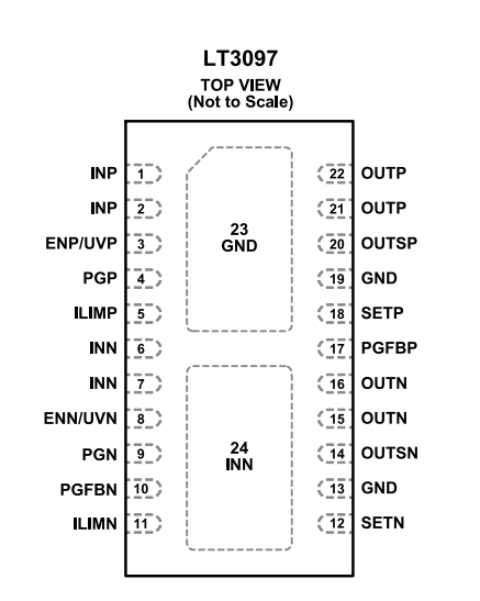
Pin layout:
- Left side: Positive LDO (INP → OUTP)
- Right side: Negative LDO (INN → OUTN)
- Middle: Control & GND
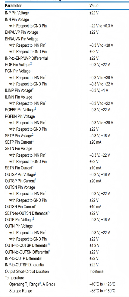
LT3097 Absolute Maximum Ratings
LT3097 Applications
1. Bipolar ultra-low noise power supply
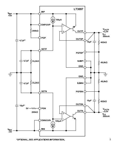
The LT3097 simultaneously offers ultra-low noise (in the μVrms range) and high PSRR (suppressing power supply ripple), so a single chip can provide both positive and negative power supplies. It can reduce the number of components, improve system consistency, and reduce noise interference. It is commonly used in applications such as operational amplifiers, precision analog front-ends, and audio systems.
2. RF radio frequency power supply
RF systems are extremely sensitive to power supply noise. Power supply ripple directly leads to phase noise degradation, signal distortion, and an increase in communication bit error rate. The advantage of the LT3097 is its extremely high PSRR and extremely low output noise, which can effectively improve the signal purity and stability of the RF link.
3. Low-noise instrument
In scenarios such as oscilloscopes, optical measurement equipment, and laboratory instruments, the measurement accuracy of instruments is often limited by power supply noise. The role of the LT3097 is to provide "clean power" and reduce measurement errors.
4. High-speed/high-precision data converter
The noise of the LT3097 is stable and does not change with the output voltage, and it has high PSRR to suppress interference from upstream switching power supplies. This effectively solves the problem that power supply noise can directly affect ENOB and SNR.
5. Medical applications: Imaging and diagnosis
Commonly used equipment such as CT/MRI or ultrasound devices and biological signal detection all require extremely low noise, high stability, and high reliability. The LT3097 can provide precise power supply and has multiple protection mechanisms, ensuring the accuracy of medical data and equipment safety.
6. Precision power supply
In applications such as reference power supplies, calibration systems, and industrial control, there is a need for stable output and low drift, low noise. The LT3097 has the advantage of allowing error amplifiers to operate at unit gain and having performance that does not change with voltage.
7. Post-switch power supply stabilization
When used as a switch power supply, the LT3097 can purify the output voltage by suppressing residual ripple and high-frequency switching noise. This hybrid architecture combines the high efficiency of switching regulators with the low noise performance of linear regulators. Therefore, the LT3097 can achieve both efficiency and low noise.
LT3097 Design advantages
- One chip handles both positive and negative power supplies (saving space)
- Extremely low noise → suitable for high-end analog systems
- High PSRR → strong ability to suppress ripple in switching power supply
- Simple periphery → only 1 resistor + capacitor are needed for each path
Notes for Using LT3097
- Output capacitor ≥ 10µF ceramic capacitor
- Attention should be paid to heat dissipation in PCB layout (DFN package)
- High PSRR performance depends on proper wiring
Common Issues and Practical Solutions for LT3097
1. Why is the output unstable / oscillating?Common causes:
- Insufficient output capacitor (less than 10 µF)
- Use of high ESR capacitor (or too far away in layout)
- Each output should have at least 10µF ceramic capacitor.
- The capacitor should be close to the OUT pin.
- X5R / X7R is preferred.
Common causes:
- The NR (noise reduction) pin is not connected to a capacitor.
- The power input itself has high noise.
- Add a 10nF to 100nF capacitor to the NR pin.
- The preamplifier is recommended to have LC or π-type filtering.
- Reasonably separate the analog ground from the power ground.
Common reasons:
- The current is close to the maximum value (500mA)
- The temperature is high
- Leave sufficient input margin (≥ 300 mV)
- Optimize heat dissipation (large area GND)
- Reduce load current
Common causes:
- Incorrect configuration of the SET resistor
- Different loads for the positive and negative channels
- Precisely calculate the SET resistance
- Try to make the positive and negative channels have symmetrical loads
- Ensure a single-point reference for GND
Cause analysis:
- An LDO is essentially a linear device, power consumption = (Vin - Vout) × I
- Reduce input voltage
- Use a pre-stage DC-DC to reduce voltage
- Enhance heat dissipation (DFN bottom pads)
Common causes:
- Output voltage not reaching the set value
- PG pin not properly pulled up
- Check if the output is stable
- Use an upper pull-up resistor (usually 10k)
- Confirm the SHDN logic is correct
Yes, but be aware of the following:
- Whether dual positive and negative power supplies are required
- Whether the noise requirements are the same
- Whether the pins are compatible (usually not compatible)
- Product attributes
- Attribute value
- Manufacturer:
- Analog Devices Inc.
- Series:
- -
- Package/Case:
- 22-WFDFN Exposed Pad
- Packaging:
- Tube
- Part Status:
- Active
- Resistance:
- Positive and Negative
- Tolerance:
- Adjustable
- Composition:
- ±20V
- Features:
- 0V
- Temperature Coefficient:
- 15V, -19V
- Operating Temperature:
- 0.65V @ 200mA
- Supplier Device Package:
- 500mA, 500mA
- Power (Watts):
- 2
- Ratings:
- 101 µA
- Size / Dimension:
- 102 µA
- Height - Seated (Max):
- -
- Number of Terminations:
- Current Limit, Enable, Soft Start
- Failure Rate:
- Over Current, Over Temperature, Reverse Current, Reverse Polarity, Short Circuit, Under Voltage Lockout (UVLO)
| Image | |
 |
| Part Number | LT3097ADJC#PBF | LT3097ADJC#TRPBF |
| Manufacturer | Analog Devices Inc. | Analog Devices Inc. |
| Series | - | - |
| Package/Case | 22-WFDFN Exposed Pad | 22-WFDFN Exposed Pad |
| Packaging | Tube | Tape & Reel (TR) |
| Part Status | Active | Active |
| Output Configuration | Positive and Negative | Positive and Negative |
| Output Type | Adjustable | Adjustable |
| Voltage - Input (Max) | ±20V | ±20V |
| Voltage - Output (Min/Fixed) | 0V | 0V |
| Voltage - Output (Max) | 15V, -19V | 15V, -19V |
| Qualification | - | - |
| Voltage Dropout (Max) | 0.65V @ 200mA | 0.41V @ 500mA, 0.45V @ 500mA |
| Current - Output | 500mA, 500mA | 500mA, 500mA |
| Number of Regulators | 2 | 2 |
| Current - Quiescent (Iq) | 101 µA | 101 µA |
| Current - Supply (Max) | 102 µA | 102 µA |
| Grade | - | - |
| PSRR | - | 108dB ~ 28dB (120Hz ~ 10MHz), 117dB ~ 53dB (120Hz ~ 10MHz) |
| Mounting Style | Surface Mount | Surface Mount |
| Operating Temperature | -40°C ~ 125°C (TJ) | -40°C ~ 125°C (TJ) |
| Control Features | Current Limit, Enable, Soft Start | Current Limit, Enable, Soft Start |
| Protection Features | Over Current, Over Temperature, Reverse Current, Reverse Polarity, Short Circuit, Under Voltage Lockout (UVLO) | Over Current, Over Temperature, Reverse Current, Reverse Polarity, Short Circuit, Under Voltage Lockout (UVLO) |
| Supplier Device Package | 22-DFN (6x3) | 22-DFN (6x3) |
inventory:2,183
Please send an inquiry. Send us your inquiry, and we will respond immediately.
-
MIC5504-1.8YM5-TR
Microchip Technology
-
MIC5504-3.3YM5-TR
Microchip Technology
-
MIC5365-3.0YC5-TR
Microchip Technology
-
MIC5365-1.8YC5-TR
Microchip Technology
-
MIC5365-2.5YC5-TR
Microchip Technology
-
MIC5365-3.3YC5-TR
Microchip Technology

- Fast Shipping Fast and convenient door to door delivery.

- Paypment Security More than 5 different secure payment methods.

- Strictly Quality Control 365 days After-Sales Service and Warranty

- Simple And Professional One-stop Electronics Procurement Solutions.