LTC2412: The Ideal Choice for High-Precision Dual-Channel 24-Bit ΔΣ ADC

- Part No.:
- LTC2412CGN#PBF
- Manufacturer:
- Analog Devices Inc.
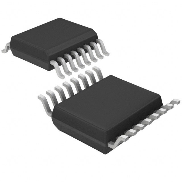
- Package:
- 16-SSOP (0.154", 3.90mm Width)
- Description:
- IC ADC 24BIT SIGMA-DELTA 16SSOP
- Quantity:
- Payment:

- Shipping:

Article Details
- Details
- Specifications
- Comparison
In the field of high-precision analog signal acquisition, the resolution, noise performance and anti-interference ability of the analog-to-digital converter often determine the overall measurement accuracy of the system. The LTC2412 is precisely such a Delta-Sigma-ADC that can provide 24-bit resolution on two differential inputs and is widely used in industrial measurement and precision instruments.
Understanding LTC2412
Decomposition of LRC2412 chip
The chip size of LTC2412 is 3.1 mm x 2.0 mm. The left area of the chip integrates typical logic structures to achieve control and digital filtering functions. The digital interface is located at the lower edge of the chip, surrounded by two grounding pads on both sides. Three differential input terminals are placed at the upper edge. On the right area of the chip, there are three larger symmetrical structures, which have larger capacitance values and might be three differential sigma modulators.
The main parameters of LTC2412 in the data sheet
The data sheet indicates that the integral non-linearity of LTC2412 is 2ppm, the full-scale deviation is 2.5ppm, the offset is 0.1ppm, the root mean square noise is 0.16ppm, and it has extremely high accuracy and stability. These are just typical values and not the maximum values. The internal oscillator operates at a frequency of 19.2kHz. The maximum external clock can reach 500kHz. At this time, the conversion time is 41 milliseconds. Under a supply voltage of 2.7V to 5.5V, LTC2412 consumes only 200 microamps of current during normal operation.
The block diagram in the data table illustrates the integrated functions of the LTC2412. The two differential inputs are switched to the input of the ΔΣ analog-to-digital converter through a multiplexer. The reference voltage is also provided in a differential manner. This ADC is a third-order ΔΣ modulator, which means that three modulators are connected in series, thereby improving the signal-to-noise ratio. Before the final serial output data, there is a digital filter. The internal clock can be configured to filter out 50Hz or 60Hz interference as much as possible.
ABSOLUTE MAXIMUM RATINGS

Using LTC2412
The LTC2412 is a high-performance ADC. For engineering applications that require high-resolution measurements, strict power-frequency suppression, and low-power consumption, the LTC2412 needs to achieve high-precision and low-noise signal conversion. Its core working process is divided into four stages: signal acquisition - ΔΣ modulation - digital filtering - data output.1. Differential Input and Channel Switching Mechanism
The LTC2412 has two differential input channels. When the chip is operating, it automatically alternates between the two channels for sampling and conversion, without the need for external control of the multiplexer. After each conversion is completed, the output data will include a channel ID identifier, allowing the master control system to easily distinguish which channel the current data comes from.
2. Delta-Sigma Modulation Principle
After the analog signal enters the ADC, the LTC2412 oversamples the input signal and uses the ΔΣ modulator to convert the continuous analog voltage into a high-speed bit stream of one or more bits, achieving a 24-bit resolution and extremely low noise.
3. No Latency Digital Filtering
The LTC2412 adopts a non-delay digital filtering structure, characterized by:
- One conversion yields completely stable data
- No need to discard previous results after channel switching
- Perfect for multi-channel polling measurement
The digital filter of the LTC2412 deeply suppresses 50Hz or 60Hz power frequency noise. Through a single pin configuration, it selects the 50Hz or 60Hz (±2%) suppression mode, achieving an differential mode suppression ratio of over 110dB at the target frequency.
5. Voltage Input and Common Mode Control
The conversion result of the LTC2412 is a proportional value relative to the external reference voltage VREF:
- Supports differential reference voltages ranging from 0.1V to VCC
- The full-scale input range is from -0.5VREF to +0.5VREF
- Input common mode voltage (VINCM)
- Reference common mode voltage (VREFCM)
6. Data Output and Communication Process
After a conversion is completed, the LTC2412 outputs 24-bit conversion data and channel information through a three-wire serial interface:
- Interface compatible with SPI/MICROWIRE
- Simple communication structure, flexible timing
- Easy to connect with MCU, FPGA
LTC2412 Application Example
With its high precision, low noise and strong anti-interference capability, the LTC2412 is particularly suitable for the following scenarios:
- Direct Sensor Digitizern
- Weight Scalesn
- Direct Temperature Measurementn
- Gas Analyzersn
- Strain-Gage Transducersn
- Instrumentationn
- Data Acquisitionn
- Industrial Process Controln
- 6-Digit DVMs

FAQ about LTC2412
1. Is the LTC2412 suitable for measuring DC or AC signals?The LTC2412 is mainly suitable for DC and low-frequency signal measurements. Its ΔΣ architecture and deep digital filtering offer extremely high accuracy for low-frequency and DC signals, and are not suitable for high-speed or high-frequency AC signal sampling.
2. Why does the LTC2412 particularly emphasize 50Hz/60Hz suppression?
In industrial and instrumentation applications, power frequency interference is the most common noise source. The LTC2412 can achieve a differential mode suppression ratio of >110dB at 50Hz or 60Hz (±2%).
3. What is No Latency? What are the benefits?
No latency means:
- Each conversion result is completely stable
- No data needs to be discarded after channel switching
- Improving the utilization of effective data
- Very suitable for multi-channel polling sampling
- Simplifying software processing logic
- Product attributes
- Attribute value
- Manufacturer:
- Analog Devices Inc.
- Series:
- microPOWER™
- Package/Case:
- 16-SSOP (0.154", 3.90mm Width)
- Packaging:
- Tube
- Part Status:
- Active
- Resistance:
- 24
- Tolerance:
- 7.5
- Composition:
- Differential
- Features:
- SPI
- Temperature Coefficient:
- MUX-ADC
- Operating Temperature:
- -
- Supplier Device Package:
- 1
- Power (Watts):
- 2
- Ratings:
- Sigma-Delta
- Size / Dimension:
- External
- Height - Seated (Max):
- 2.7V ~ 5.5V
- Number of Terminations:
- 2.7V ~ 5.5V
- Failure Rate:
- -
| Image | |
 |
| Part Number | LTC2412CGN#PBF | LTC2412CGN#TRPBF |
| Manufacturer | Analog Devices Inc. | Analog Devices Inc. |
| Series | microPOWER™ | microPOWER™ |
| Package/Case | 16-SSOP (0.154", 3.90mm Width) | 16-SSOP (0.154", 3.90mm Width) |
| Packaging | Tube | Tape & Reel (TR) |
| Part Status | Active | Active |
| Number of Bits | 24 | 24 |
| Sampling Rate (Per Second) | 7.5 | 7.5 |
| Input Type | Differential | Differential |
| Data Interface | SPI | SPI |
| Configuration | MUX-ADC | MUX-ADC |
| Mounting Style | Surface Mount | Surface Mount |
| Ratio - S/H:ADC | - | - |
| Number of A/D Converters | 1 | 1 |
| Number of Inputs | 2 | 2 |
| Architecture | Sigma-Delta | Sigma-Delta |
| Reference Type | External | External |
| Supplier Device Package | 16-SSOP | 16-SSOP |
| Voltage - Supply, Analog | 2.7V ~ 5.5V | 2.7V ~ 5.5V |
| Grade | - | - |
| Operating Temperature | 0°C ~ 70°C | 0°C ~ 70°C |
| Voltage - Supply, Digital | 2.7V ~ 5.5V | 2.7V ~ 5.5V |
| Features | - | - |
| Qualification | - | - |
inventory:4,468
Please send an inquiry. Send us your inquiry, and we will respond immediately.
-
ADC081C021CIMKX/NOPB
Texas Instruments
-
MCP3021A5T-E/OT
Microchip Technology
-
TLA2024IRUGR
Texas Instruments
-
MCP3221A5T-E/OT
Microchip Technology
-
MCP3221A5T-I/OT
Microchip Technology
-
MCP3221A4T-E/OT
Microchip Technology

- Fast Shipping Fast and convenient door to door delivery.

- Paypment Security More than 5 different secure payment methods.

- Strictly Quality Control 365 days After-Sales Service and Warranty

- Simple And Professional One-stop Electronics Procurement Solutions.