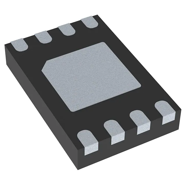
MT29F2G01ABAGDWB-IT:G --2Gb SLC SPI NAND Flash
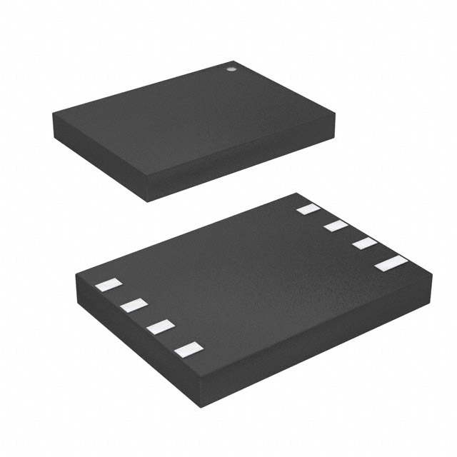
- Part No.:
- MT29F2G01ABAGDWB-IT:G
- Manufacturer:
- Micron Technology Inc.
- Package:
- 8-UDFN
- Description:
- IC FLASH 2GBIT SPI 8UPDFN
- Quantity:
- Payment:

- Shipping:

Article Details
- Details
- Specifications
- Comparison
Introduction
MT29F2G01ABAGDWB-IT:G is a 2Gbit NAND Flash memory that supports SPI interface. It has an 8-pin U-PDFN package with low pin count, making it suitable for space-constrained embedded or industrial systems. It is suitable for applications in embedded systems, industrial equipment, and scenarios requiring high reliability and durability storage.
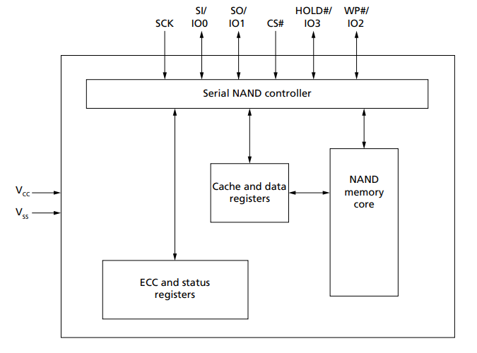
Datasheet keys
- Storage density: 2 Gbit (2 G × 1)
- Interface type: SPI (standard/extended SPI)
- Maximum clock frequency: ≈ 133 MHz
- Voltage range (VCC): 2.7 V - 3.6 V
- Package: 8-pin U-PDFN
- Temperature range: -40 °C to +85 °C (industrial grade)
- Durability: 100,000 program/erase cycles (typical)
- Data retention period (unwritten): 10 years (at 85 °C)
Features
- Single-level cell (SLC) technology
- 2Gb density
- Organization
- Page size x1: 2176 bytes (2048 + 128 bytes)
- Block size: 64 pages (128K + 8K bytes)
- Plane size: 2Gb (2 planes, 1024 blocks per plane)
- Standard and extended SPI-compatible serial businterface
- Instruction, address on 1 pin; data out on 1, 2, or4 pins
- Instruction on 1 pin; address, data out on 2 or 4pins
- Instruction, address on 1 pin; data in on 1 or 4pins
- User-selectable internal ECC supported– 8 bits/sector
- Array performance
- 133 MHz clock frequency (MAX)
- Page read: 25µs (MAX) with on-die ECC disabled;70µs (MAX) with on-die ECC enabled
- Page program: 200µs (TYP) with on-die ECC disabled; 220µs (TYP) with on-die ECC enabled
- Block erase: 2ms (TYP)
- Advanced features
- Read page cache mode
- Read unique ID
- Read parameter page
- Device initialization
- Automatic device initialization after power-up
- Security
- Blocks 7:0 are valid when shipped from factorywith ECC enabled
- Software write protection with lock register
- Hardware write protection to freeze BP bits
- Lock tight to freeze BP bits during one power cycle
- Permanent block lock protection
- OTP Space: 10 pages one-time programmableNAND Flash memory area
- Operating voltage range
- VCC = 2.7–3.6V
- Operating temperature
- Industrial: –40°C to +85°C
- Quality and reliability
- Endurance: 100,000 PROGRAM/ERASE cycles
- Data retention: JESD47H-compliant; see qualification report
- Additional: Uncycled data retention: 10 years24/7 @85°C
- Package
- 16-pin SOP, 300 mils (package code: SF)
- 8-pin U-PDFN, 8mm x 6mm x 0.65mm (MLP8)(package code: WB)
- 24-ball T-PBGA, 05/6mm x 8mm (5 x 5 array)(package code: 12)
Packaging, Pins
- Packaging: U-PDFN-8 (6 × 8 mm) surface mount
- Note: ESD protection, re-etch sensitivity (MSL)
- Attention to signal integrity and layout of power/ground planes during wiring.
- The bottom of the package needs a heat dissipation or grounding pad to ensure complete thermal management and grounding.
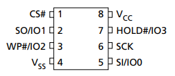
Working Principle
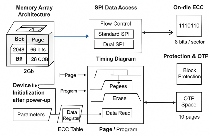
1. Storage Array Structure
Inside the chip, it is composed of the NAND Flash standard structure:- Page = 2048B data + 128B OOB
- Block = 64 Pages Plane = 1024 Blocks
- Full chip 2Gb = 2 Planes
2. SPI Data Access
MT29F2G01ABAGDWB-IT:G uses standard SPI / Dual SPI / Quad SPI access methods.Read process: Page → Data Register
Data Register → SPI Output
Writing Process:
Write data to the internal Data Register (SPI)
Program Execution: Write the data in the register to the Page
Erase Process:
Issue the BLOCK ERASE command
The Flash will restore all bits of the entire Block to "1"
3. Built-in ECC
- Correct bit errors caused by storage aging
- Improve data reliability
- Extend system lifespan
4. Security and Protection
1) Write Protection- Software locks the register
- The hardware WP# pin can freeze the BP bit
- Lock Tight: Completely lock within one power-on cycle
- Fixed 10 pages
- Cannot be modified after program writing
- Suitable for writing serial numbers, check codes, etc.
5. Power-on Initialization
- Execute the internal initialization sequence
- Read the parameter page
- Reload the ECC table
- Enter the standby accessible state
Design Considerations
- For use in MCU/Embedded Systems, it is necessary to confirm that the MCU/controller supports the command set of this SPI NAND.
- NAND has block-level management requirements, so the software needs to have Bad Block Management, wear-leveling, and block locking mechanisms.
- For high-reliability requirements (such as industrial, automotive-grade), it is recommended to consider temperature-induced degradation, data retention capability, and the manufacturer's reliability certification report.
- When purchasing, it is necessary to confirm that the complete part number suffix (such as "IT:G") corresponds to the function, version, and package with the design.
Conclusion
MT29F2G01ABAGDWB-IT:G: It performs read, write, and erase operations in the NAND array with a Page/Block structure through the SPI interface. It ensures high reliability of data storage by using built-in ECC and protection mechanisms, and is highly suitable for embedded systems, industrial equipment, and storage scenarios requiring high reliability/longevity (SLC outperforms MLC/QLC).- Product attributes
- Attribute value
- Manufacturer:
- Micron Technology Inc.
- Series:
- -
- Package/Case:
- 8-UDFN
- Packaging:
- Tray
- Part Status:
- Active
- Resistance:
- Verified
- Tolerance:
- Non-Volatile
- Composition:
- FLASH - NAND
- Features:
- 2Gbit
- Temperature Coefficient:
- 2G x 1
- Operating Temperature:
- SPI
- Supplier Device Package:
- -
- Power (Watts):
- FLASH
- Ratings:
- -
- Size / Dimension:
- -
- Height - Seated (Max):
- 2.7V ~ 3.6V
- Number of Terminations:
- -40°C ~ 85°C (TA)
- Failure Rate:
- -
| Image |  |
 |
| Part Number | MT29F2G01ABAGDWB-IT:G TR | MT29F2G01ABAGDWB-IT:G |
| Manufacturer | Micron Technology Inc. | Micron Technology Inc. |
| Series | - | - |
| Package/Case | 8-UDFN | 8-UDFN |
| Packaging | Tape & Reel (TR) | Tray |
| Part Status | Active | Active |
| Programmable | Verified | Verified |
| Memory Type | Non-Volatile | Non-Volatile |
| Technology | FLASH - NAND | FLASH - NAND |
| Memory Size | 2Gbit | 2Gbit |
| Memory Organization | 2G x 1 | 2G x 1 |
| Supplier Device Package | 8-UPDFN (8x6) (MLP8) | 8-UPDFN (8x6) (MLP8) |
| Memory Interface | SPI | SPI |
| Clock Frequency | - | - |
| Memory Format | FLASH | FLASH |
| Write Cycle Time - Word, Page | - | - |
| Access Time | - | - |
| Mounting Style | Surface Mount | Surface Mount |
| Voltage - Supply | 2.7V ~ 3.6V | 2.7V ~ 3.6V |
| Qualification | - | - |
| Operating Temperature | -40°C ~ 85°C (TA) | -40°C ~ 85°C (TA) |
| Grade | - | - |
inventory:1,834
Please send an inquiry. Send us your inquiry, and we will respond immediately.
-
M24C02-WMN6TP
STMicroelectronics
-
AT24C02C-XHM-T
Microchip Technology

-
AT21CS01-STUM10-T
Microchip Technology
-
AT24C02C-SSHM-T
Microchip Technology
-
24LC01BT-I/OT
Microchip Technology
-
M24C02-FMC6TG
STMicroelectronics


