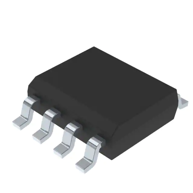
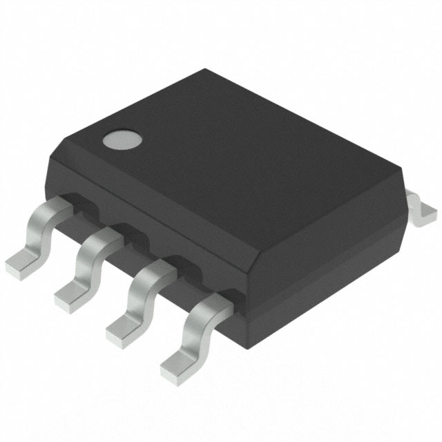
W25Q64JVSSIQ - A high-speed, low-power 64Mb SPI NOR Flash memory storage solution

- Part No.:
- W25Q64JVSSIQ
- Manufacturer:
- Winbond Electronics
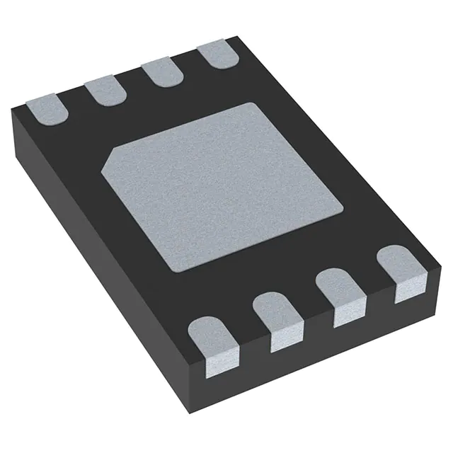
- Package:
- 8-SOIC (0.209", 5.30mm Width)
- Description:
- IC FLASH 64MBIT SPI/QUAD 8SOIC
- Quantity:
- Payment:

- Shipping:

Article Details
- Details
- Specifications
- Comparison
Introduction
The W25Q64JVSSIQ is a 64M-bit serial flash memory chip in the W25Q64JV series, featuring an SOIC-8 package, an industrial temperature range, and tape packaging. It supports SPI and dual/quad SPI interfaces, with a maximum SPI clock frequency of 133MHz and a data transfer rate of up to 532MHz in Quad I/O mode. The device operates within a voltage range of 2.7V to 3.6V and has a low power consumption of 1µA in power-down mode. It contains 32,768 programmable pages (256 bytes per page) and supports 4KB sectors, 32KB blocks, 64KB blocks, and full-chip erasure. It has 2,048 erasable sectors and 128 erasable blocks, providing a flexible solution for data and parameter storage. The device supports JEDEC standard manufacturer and device IDs, a 64-bit unique serial number, and three 256-byte security registers, making it widely applicable in code storage, embedded systems, consumer electronics, and industrial control applications.
This article will describe the features, application examples, key information in the datasheet, working principle, and design concept of the W25Q64JVSSIQ.
FEATURES
- New Family of SpiFlash Memories
- W25Q64JV: 64M-bit / 8M-byte
- Standard SPI: CLK, /CS, DI, DO
- Dual SPI: CLK, /CS, IO0, IO1
- Quad SPI: CLK, /CS, IO0, IO1, IO2, IO3
- Software & Hardware Reset(1)
- Highest Performance Serial Flash
- 133MHz Single, Dual/Quad SPI clocks266/532MHz equivalent Dual/Quad SPI
- Min. 100K Program-Erase cycles per sector
- More than 20-year data retention
- Efficient "Continuous Read"
- Continuous Read with 8/16/32/64-Byte Wrap
- As few as 8 clocks to address memory
- Allows true XIP (execute in place) operation
- Outperforms X16 Parallel Flash
- Low Power, Wide Temperature Range
- Single 2.7 to 3.6V supply
- <1µA Power-down (typ.)
- -40°C to +85°C operating range
- Flexible Architecture with 4KB sectors
- Uniform Sector/Block Erase (4K/32K/64K-Byte)
- Program 1 to 256 byte per programmable page
- Erase/Program Suspend & Resume
- Advanced Security Features
- Software and Hardware Write-Protect
- Special OTP protection(1)
- Top/Bottom, Complement array protection
- Individual Block/Sector array protection
- 64-Bit Unique ID for each device
- Discoverable Parameters (SFDP) Register
- 3X256-Bytes Security Registers
- Volatile & Non-volatile Status Register Bits
- Space Efficient Packaging
- 8-pin SOIC 208-mil / VSOP 208-mil
- 8-pad WSON 6x5-mm/8x6-mm, XSON 4x4-mm
- 16-pin SOIC 300-mil
- 8-pin PDIP 300-mil
- 24-ball TFBGA 8x6-mm (6x4 ball array)
- 24-ball TFBGA 8x6-mm (6x4/5x5 ball array)
- Contact Winbond for KGD and other options
Working Principle
The data transmission methods, reset mechanisms, and multiple write protection mechanisms of W25Q64JVSSIQ in different SPI modes can be classified into five core functional points:- Standard SPI instructions
- Dual SPI instructions
- Quad SPI instructions
- Software reset and hardware reset pins
- Write protection
The device supports software reset (66h + 99h) and hardware reset (/RESET pin), which can quickly restore to the default state in case of system anomalies or during power-on initialization, ensuring stable operation.
In terms of data security, W25Q64JVSSIQ has a complete write protection mechanism. The chip can prevent accidental writing or interference through various methods such as status registers, block/sector locking, power-off protection, and one-time programmable (OTP). After power-on, it automatically enters a write-disabled state and requires a write enable instruction (Write Enable) to perform programming or erasing operations.

Applications
- Microcontroller firmware storage (MCU code storage)
- Industrial control system
- Consumer electronic products (televisions, set-top boxes, audio equipment, etc.)
- Computer BIOS storage
- Firmware and data cache of Internet of Things devices
Datasheet Highlights
- Package: SOIC-8
- Interface type: SPI
- Storage capacity: 64Mbit
- Clock frequency: 133MHz
- Operating voltage: 2.7V - 3.6V

Design Considerations
- Compatibility and Standardized Design: Fully compatible with standard SPI, Dual SPI, and Quad SPI interfaces, supporting mainstream microcontrollers and SoCs.
- High Performance and Flexibility: Offers high-speed reading and writing, scalable instruction set, and supports XIP (Execute In Place) direct execution.
- Low Power Consumption and Reliability: Utilizes low-power architecture and power-off protection design, suitable for battery-powered devices.
- Multi-level Security and Write Protection Mechanism: Provides multi-level write protection, block locking, power-off write protection, software reset, etc., to ensure data security.
- Wide Adaptability of Packaging and Capacity Design: Offers SOP-8, WSON, TFBGA, etc. packaging, facilitating system design integration.
Conclusion
The W25Q64JVSSIQ, with its multi-level SPI transmission mode, high-speed read-write performance and reliable data protection features, featuring high compatibility, low power consumption and high-speed access, is a universal SPI Flash solution for multi-application platforms. It is highly suitable for code storage, firmware update, consumer electronics and industrial control fields.- Product attributes
- Attribute value
- Manufacturer:
- Winbond Electronics
- Series:
- SpiFlash®
- Package/Case:
- 8-SOIC (0.209", 5.30mm Width)
- Packaging:
- Tube
- Part Status:
- Active
- Resistance:
- Verified
- Tolerance:
- Non-Volatile
- Composition:
- FLASH - NOR
- Features:
- 64Mbit
- Temperature Coefficient:
- 8M x 8
- Operating Temperature:
- SPI - Quad I/O
- Supplier Device Package:
- 133 MHz
- Power (Watts):
- FLASH
- Ratings:
- 3ms
- Size / Dimension:
- -
- Height - Seated (Max):
- 2.7V ~ 3.6V
- Number of Terminations:
- -40°C ~ 85°C (TA)
- Failure Rate:
- -
| Image | |
|
| Part Number | W25Q64JVSSIQ | W25Q64JVSSIQ TR |
| Manufacturer | Winbond Electronics | Winbond Electronics |
| Series | SpiFlash® | SpiFlash® |
| Package/Case | 8-SOIC (0.209", 5.30mm Width) | 8-SOIC (0.209", 5.30mm Width) |
| Packaging | Tube | Tape & Reel (TR) |
| Part Status | Active | Active |
| Programmable | Verified | Verified |
| Memory Type | Non-Volatile | Non-Volatile |
| Technology | FLASH - NOR | FLASH - NOR |
| Memory Size | 64Mbit | 64Mbit |
| Memory Organization | 8M x 8 | 8M x 8 |
| Supplier Device Package | 8-SOIC | 8-SOIC |
| Memory Interface | SPI - Quad I/O | SPI - Quad I/O |
| Clock Frequency | 133 MHz | 133 MHz |
| Memory Format | FLASH | FLASH |
| Write Cycle Time - Word, Page | 3ms | 3ms |
| Access Time | - | - |
| Mounting Style | Surface Mount | Surface Mount |
| Voltage - Supply | 2.7V ~ 3.6V | 2.7V ~ 3.6V |
| Qualification | - | - |
| Operating Temperature | -40°C ~ 85°C (TA) | -40°C ~ 85°C (TA) |
| Grade | - | - |
inventory:22,088
Please send an inquiry. Send us your inquiry, and we will respond immediately.
-
M24C02-WMN6TP
STMicroelectronics
-
AT24C02C-XHM-T
Microchip Technology
-
AT21CS01-STUM10-T
Microchip Technology
-
AT24C02C-SSHM-T
Microchip Technology
-
24LC01BT-I/OT
Microchip Technology
-
M24C02-FMC6TG
STMicroelectronics

- Fast Shipping Fast and convenient door to door delivery.

- Paypment Security More than 5 different secure payment methods.

- Strictly Quality Control 365 days After-Sales Service and Warranty

- Simple And Professional One-stop Electronics Procurement Solutions.