Hello! now
 +8619886240609(Bella)
China's first innovation opens up new space for heat dissipation of high-power semiconductor chips.
1/21/2026 12:25:13 AM
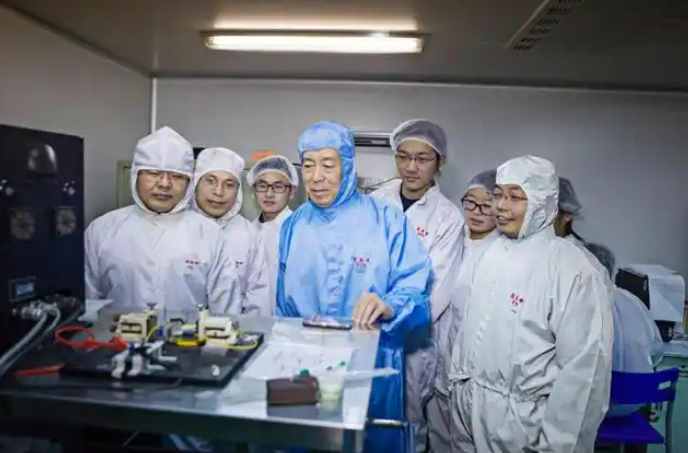
Recently, a team led by Academician Hao Yue and Professor Zhang Jincheng from Xidian University has successfully transformed the rough "island-like" interface into an atomically smooth "film" through innovative technology, achieving a breakthrough improvement in chip heat dissipation efficiency and device performance. This breakthrough achievement, which provides a "Chinese model" for the high-quality integration of semiconductor materials, has been published in authoritative journals such as 《Nature Communications》and《Science Advances》.
The "thermal bottleneck" that has long constrained the performance of RF chips
"Traditional semiconductor chips have a rough surface on the crystal nucleation layer, which seriously affects the heat dissipation effect," said Professor Zhang Jincheng, vice president of Xidian University. "If the heat cannot be dissipated, it will form 'thermal hotspots', which can lead to a decline in chip performance or even device damage in severe cases." Although the related nucleation technology won the Nobel Prize in 2014, the heat dissipation problem caused by the rough interface has not been completely solved, becoming the core bottleneck for further upgrading of high-frequency and high-power RF devices.Aluminum nitride film technology brings performance leap
Based on this innovative aluminum nitride film technology, the research team has achieved significant breakthroughs in the performance of gallium nitride microwave power devices in multiple frequency bands:- Output power density of 42 W/mm in the X-band
- Output power density of 20 W/mm in the Ka-band
Deep impact on communication and future applications
For communication base stations, it can achieve a longer signal coverage and lower energy consumption. The more profound impact lies in that it reserves the key core device capabilities for promoting the development of future industries such as 5G/6G communication and satellite internet.- Radar and detection systems: Significantly improved detection range and resolution under the same volume and power consumption conditions
- 5G/6G communication base stations: Achieve a longer coverage range and lower overall energy consumption
- Satellite communication and satellite internet: Improve link stability and system efficiency
Semiconductor materials: The underlying support of the chip industry
Semiconductor materials are the cornerstone of chip manufacturing and are important materials for making integrated circuits, discrete devices, sensors, optoelectronic devices, and other products. From photoresist to silicon wafers, from electronic gases to CMP polishing pads, semiconductor materials are hailed as the "food" of the chip industry.TECHCET predicts that the global semiconductor materials market size will reach approximately 70 billion US dollars in 2025, with a year-on-year growth of 6%. The same institution also predicts that the semiconductor materials market size will exceed 87 billion US dollars in 2029. Domestically, according to statistics and predictions by the China Business Industry Research Institute, the market size of key materials in China will reach 174.1 billion yuan in 2025, with a year-on-year growth of 21.1%.
Key opportunities
Under the current complex international environment, the localization of semiconductor materials may accelerate. Technological breakthroughs represented by aluminum nitride and gallium nitride, the third-generation semiconductor materials, not only enhance device performance but also provide a practical path for the autonomy and control of the industrial chain.With the rapid development of advanced processes, storage, and packaging, coupled with the strong promotion of localization policies, semiconductor localization materials are facing important development opportunities.
Related information


- Fast Shipping Fast and convenient door to door delivery.

- Paypment Security More than 5 different secure payment methods.

- Strictly Quality Control 365 days After-Sales Service and Warranty

- Simple And Professional One-stop Electronics Procurement Solutions.